Full Suite of Microfabrication Technologies
Mutech Microsystems μLaser, μAligner, μCoater, and μExposer
Mutech Microsystems is focused on the development of systems and equipment for the promotion of science, technology, and education in the areas of microfabrication, along with micro and nano mechanics and electronics. They develop and manufacture high-tech equipment to improve the access of new technology to the productive sectors of research and development. From their headquarters in San Carlos de Bariloche, Río Negro, Argentina, they develop microfabrication equipment that increases the capabilities and technological level of any nanotechnology laboratory. Products include direct laser lithography, mask aligners, spin coaters, and exposure tools.
Models
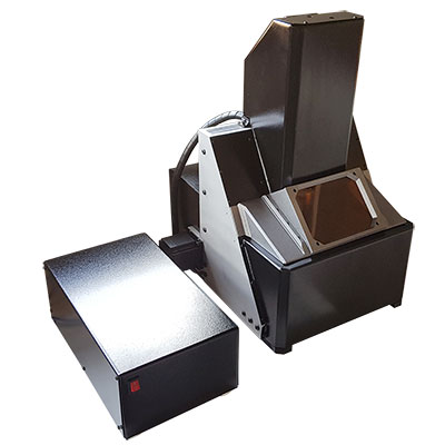
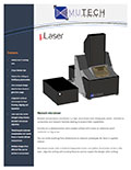
μLaser
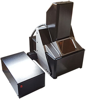
μLaser is a direct laser lithography writer, oriented to universities and research facilities looking to expand their capabilities. It writes on a photosensitive resist coated surface with a 405 nm laser at submicron pixel resolution. You can write anything from photomasks to research prototypes for basic or applied science. The integrated camera can be used to align the writing with existing features.
Optimized for ease of use and simple maintenance, direct laser lithography greatly reduces costs and execution times in areas such as microfluidics, microelectronics, micromechanics, and material science research, by eliminating the dependence of external suppliers for the production of photomasks.
FEATURES
- High resolution lithography
- Large writing area
- Spot size can be changed using included objectives
- User-friendly software
- Compact size
SPECIFICATIONS
- Typical writing speed: 100-120 mm/s
- Maximum area: 100x92 mm2
- Unidirectional positioning step: X = 0.16 µm, Y = 1.00 µm
- Raster steps of objectives: Fine 0.8 µm; Medium Fine 0.96 µm; Medium 2 µm; Coarse 5 µm
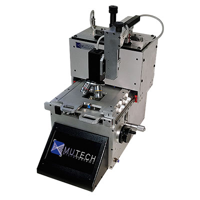
μAligner
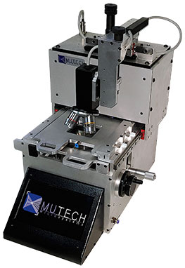
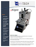
μAligner is a compact UV mask aligner designed for microfabrication applications. It allows for easy fabrication of multilayer devices on a multitude of photoresists, with excellent exposure quality. The 7-inch touchscreen is easy to use and allows alignment using the calibrated digital microscope and the X-Y-R micrometer-based alignment stage. The fully electronic wafer pressure and gap control allows for easy alignment and very high repeatability of the exposure conditions between processes.
μAligner is ideal for the fabrication of high-level systems for research applications. Main applications range from microfluidics, optics, biotechnology, and microelectronic devices. It provides the user with fast multilayer device fabrication capabilities thanks to its high resolution and high accuracy alignment.
FEATURES
- 365 nm LED source
- Large exposure area
- Electronic pressure and gap control
- Digital microscope
- Compact size
SPECIFICATIONS
- X-Y-R Aligning Stage
- Accuracy: 1 µm
- X-Y alignment span: 6 mm
- R alignment span: 5º
- Z Wafer Stage
- Stage step: 0.31 µm/step
- Pressure sensing resolution: 20 g
- Maximum pressure: 5 kg
- UV Optics
- Wavelength: 365 nm
- Exposure time: 0.1 - 200 s
- Exposure area: 100 mm diameter
- Power density: 0.2 - 20 mW/cm2
- Homogeneity: < 5%
- Light divergence: < 3°
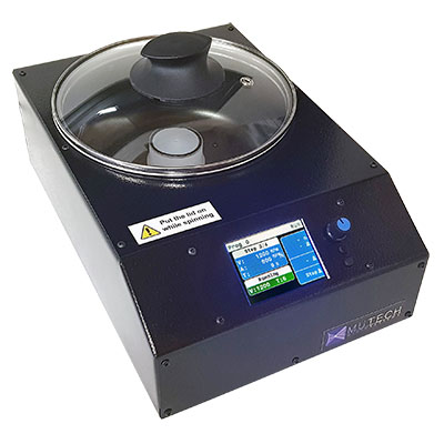
μCoater
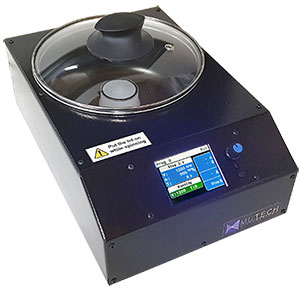
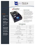
µCoater is easy to use and full of features for a benchtop spin coater. It includes an integrated vacuum system with a rotating vacuum chuck for holding the substrates to coat while spinning. You don't need an external vacuum pump as it is integrated inside. It has an all-metal body construction (steel and aluminum) with a polypropylene vacuum chuck; the inside of the spinning bowl is coated with a PTFE based material which is very easy to clean. µCoater uses a high-quality outrunner brushless motor which are very efficient and have very low static friction resulting in a long lifetime.
The µCoater has a full color TFT LCD screen with a very simple and uncluttered GUI where you can save multiple spinning programs. Each program can have several spinning steps with different speeds, accelerations and spinning times per step. The vacuum pump is also controlled from the user interface.
The spin coating process is one of the best ways to deposit thin films of coating materials on substrates. Usually a small amount of the coating material is applied on the center of a substrate and then it is rotated at high speed in a controlled manner, resulting in a homogeneous film on the substrate. This technology is typically used for the application of photosensitive materials for microfabrication applications, for the deposit of nanoparticles and nanotubes or for sol-gel processes.
FEATURES
- Integrated vacuum
- Brushless motor
- User-friendly GUI and software
SPECIFICATIONS
- Max speed: 10,000 rpm
- Min speed: 500 rpm
- Max acceleration: 5,000 rpm/s
- Max time per step: 1,000 s
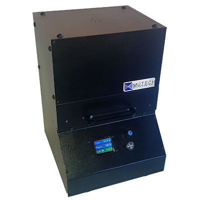
μExposer
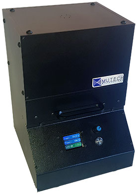
The μExposer is an UV exposing system designed for microfabrication applications. It allows the user to perform fast lithography processes on samples and substrates. The system consists of an UV 365 nm parallel LED light source and a sliding tray where you can put your photolithography mask and sample to expose. A variety of custom holders and customizations can be provided for your application.
The lithography process is the basic technique for reducing the size and dimension of devices, in the "top-bottom" approach. This technique is transversal to many fields of physics, engineering, and biosciences, expanding and consolidating microfabrication applications and nanotechnology. During the lithography process a pattern is transferred to a light sensitive resist and spin coated over the sample. The photoresist is then developed removing the exposed areas (for positive photoresists). Using chemical or physical etching (e.g., ion beam or acids attacks), the unprotected areas of the sample are removed and the desired pattern is finally transferred to the sample.
SPECIFICATIONS
- Wavelength: 365 ± 5 nm
- Exposure time: 0.1 - 100 s
- Exposure area: 100 mm diameter
- Power density: 0.2 - 20 mW/cm2
- Homogeneity: < 5%
- Light divergence: < 2°
For additional product information:
Contact Our Sales Team
